We have discussed the SMT pad of LED PCB board design, it’s a series articles about LED PCB board design.
We plan ten articles in this series, if you have any questions please let me know.
Today we are going to introduce the angle design of LED PCB board.
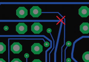
Route All Traces at 90 Degrees or Greater
Never route a circuit trace a less than a 90 degree angle.
Acute angle trace junctions can cause manufacturing problems, and can fail later.
If you need to double-back in order to complete a connection, use multiple segments.

Acute angle traces can act as acid traps, and can concentrate stress.
Re-route such corners gradually, with a series of segments.
—
From epectec, original author have all right.
Original title:TOP 10 PRINTED CIRCUIT BOARD DESIGN CHECKS
MCPCB experts recommend top 10 design tips:
- Avoid Placing Vias at the End of SMT Pads
- Do Not Route Wide Traces Into Narrow SMT Pads
- Do Not Route Traces Along Sides of SMT Pads.
- Route All Traces at 90 Degrees or Greater
- Don’t Place Components Too Close to the PCB Outline
- Never Export English-Unit Gerber or Drill Files at 2:3 Decimal Resolution
- Size Your Solder Mask Openings Consistently
- Always Use Direct Connect for Vias
- Size Your Component Hole Thermal Pads Appropriately
- Allow Enough Clearance Between Unsupported PTHs and Adjacent Copper Features on Internal Layers
