This post will discuss LED PCB board design issue.
First of all Allen wants to claim most LED PCB design content from the internet.
If you have any problems please contact us.
And this post not only focus designers, because to learn more LED PCB board design, you will understand LED PCB board more clearly, then speed your PCB project.
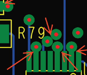
Avoid Placing Vias at the End of SMT Pads
This is especially important if the vias are not masked-over.
Placing vias too close to SMT pads will allow solder to migrate off the pad and through the via, resulting in a poor solder joint. Edge of via to edge of SMT pad should be .025” or greater whenever possible, and masking over the via pad is recommended.
Note how the mask openings for vias and SMT pads run into one another.
There is nothing to block assembly solder flow.
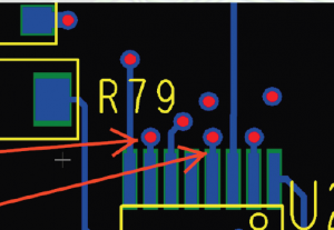
Here the openings for the SMT pads are reduced in size, and the via openings are
eliminated.
All solder will now stay on the SMT pads.
—
From epectec, original author have all right.
Original title:TOP 10 PRINTED CIRCUIT BOARD DESIGN CHECKS
MCPCB experts recommend top 10 design tips:
- Avoid Placing Vias at the End of SMT Pads
- Do Not Route Wide Traces Into Narrow SMT Pads
- Do Not Route Traces Along Sides of SMT Pads.
- Route All Traces at 90 Degrees or Greater
- Don’t Place Components Too Close to the PCB Outline
- Never Export English-Unit Gerber or Drill Files at 2:3 Decimal Resolution
- Size Your Solder Mask Openings Consistently
- Always Use Direct Connect for Vias
- Size Your Component Hole Thermal Pads Appropriately
- Allow Enough Clearance Between Unsupported PTHs and Adjacent Copper Features on Internal Layers