Previous post, we have introduced the End of SMT Pads and the Sides of SMT Pads board design.
If you haven’t read the articles above mention, Allen recommend you go back to read.
Due to this is a series posts, we are going to discus new tip of the LED PCB board design.
Size Your Solder Mask Openings Consistently
Set up your pad stack definitions so that all of your LED PCB components use the same amount of over-sizing.
Doing so will eliminate a host of design rule errors that your fabricator will need to repair before manufacturing.
Using (copper pad size +.004”) will enable your fabricator to avoid mask-on-pads, while still depositing mask material between pins of SMT components down to 0.5mm (. 0197”) pitch, with no editing. (Example: .012” x.040” copper pad, .016” x.044” solder mask opening.)

Notice the oversized openings for the vials, and the inconsistent sizing LXW of the rectangular pads.
Some openings merge.
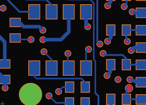
Now all mask openings are consistently and appropriately sized.
Previously overlapping openings are now separated.
—
From epectec, original author have all right.
Original title:TOP 10 PRINTED CIRCUIT BOARD DESIGN CHECKS
MCPCB experts recommend top 10 design tips:
- Avoid Placing Vias at the End of SMT Pads
- Do Not Route Wide Traces Into Narrow SMT Pads
- Do Not Route Traces Along Sides of SMT Pads.
- Route All Traces at 90 Degrees or Greater
- Don’t Place Components Too Close to the PCB Outline
- Never Export English-Unit Gerber or Drill Files at 2:3 Decimal Resolution
- Size Your Solder Mask Openings Consistently
- Always Use Direct Connect for Vias
- Size Your Component Hole Thermal Pads Appropriately
- Allow Enough Clearance Between Unsupported PTHs and Adjacent Copper Features on Internal Layers