We have discussed the End of SMT Pads and Narrow SMT Pads of LED PCB board design.
During some high-end LED PCB board, you also notice Sides of SMT Pads design.
So this post will discuss LED PCB board design Guidelines [Part 3]
How to design Sides of SMT Pads?
Do Not Route Traces Along Sides of SMT Pads.
Route traces into SMT pads midway along one edge or the other.
Some CAD systems will allow a small gap between the pad and the trace, with a short (. 005” or less) 90 degree connection to the pad.
This can act as a trap for etchant, which will continue to eat away at the trace after the rinse cycle.
In some cases, these connections will pass bare PCB continuity test, but will fail after thermal shock during assembly.
When using tight minimum spacing values, check for such connections and correct the routing manually if necessary.
Routing traces in this manner can also have the effect of creating an oversized “soldermask-defined” pad, similar to the problem caused by wide traces (described above).
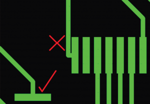
The pad marked X does not need to be routed so close to the pad.
Routing it like the checked pad will eliminate the process problem.
—
From epectec, original author have all right.
Original title:TOP 10 PRINTED CIRCUIT BOARD DESIGN CHECKS
MCPCB experts recommend top 10 design tips:
- Avoid Placing Vias at the End of SMT Pads
- Do Not Route Wide Traces Into Narrow SMT Pads
- Do Not Route Traces Along Sides of SMT Pads.
- Route All Traces at 90 Degrees or Greater
- Don’t Place Components Too Close to the PCB Outline
- Never Export English-Unit Gerber or Drill Files at 2:3 Decimal Resolution
- Size Your Solder Mask Openings Consistently
- Always Use Direct Connect for Vias
- Size Your Component Hole Thermal Pads Appropriately
- Allow Enough Clearance Between Unsupported PTHs and Adjacent Copper Features on Internal Layers