This is the last post of series articles about LED PCB board design Guidelines.
Allen wants to discuss the space between the two holes on LED PCB board.
Before we have discussed the holes design tip, but this post is different.
We will go deeper to introduce how to design a perfect hole.
Continue to read this topic.
Allow Enough Clearance Between Unsupported PTHs and Adjacent Copper Features on Internal Layers
As design rules become increasingly tighter, this DRC error is becoming more common.
Multilayer PCBs need a minimum of.006” clearance from edge of trace to barrel of the hole.
There are many factors which affect dimensional accuracy of multilayers (drill runout, material movement, artwork scaling, multiple pinning setups) so design-in at least.006”, and more whenever possible.
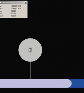
This hole is only.005” from the trace, and shows up as a min space violation.
Hole to trace needs to be.006” min (more when possible).
MCPCB experts recommend top 10 design tips:
- Avoid Placing Vias at the End of SMT Pads
- Do Not Route Wide Traces Into Narrow SMT Pads
- Do Not Route Traces Along Sides of SMT Pads.
- Route All Traces at 90 Degrees or Greater
- Don’t Place Components Too Close to the PCB Outline
- Never Export English-Unit Gerber or Drill Files at 2:3 Decimal Resolution
- Size Your Solder Mask Openings Consistently
- Always Use Direct Connect for Vias
- Size Your Component Hole Thermal Pads Appropriately
- Allow Enough Clearance Between Unsupported PTHs and Adjacent Copper Features on Internal Layers