What is Embedding Components?
Embedding Components are very newly defined for electronic designers.
That’s the reason why 4MCPCB should introduce the embedding component definition.
In some traditions PCB factories, like some Metal Core PCB factories in China, the designer follows their experience pass used.
Most of them don’t know what is embedding components, and how to design embedding component project.
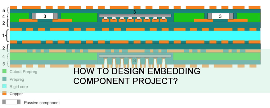
All of their projects, the printed circuit board just served as the platform for mounting.
Yes, the interconnecting acting ability is the main performance of PCB board.
And the passive components on the outer surfaces, that’s the reason why named this process as mounted components on the PCB.
Embedding component design is the electronic design trend in next 5 years
More and more smart devices have created.
If you ask the designer of those smart devices, the answer always likes below:
Most of those companies attempting to improve functionality and minimize space.
And the design processes are very different with the traditional one.
All of them will consider embedding a board range of these components within the circuit structure.
This means you should consider the mounting components process during design PCB construction.
That’s the reason why the PCB designers require higher construction knowledge than before.
The design mind of embedding components differs traditional’s
So what’s the difference between embedding components and the traditional PCB design mind.
The biggest one is the PCB construction design.
In most of traditional PCB design projects, just consider the space of the trance.
Due to the bigger space between traces, the mount components process will be easier.
But in most of smart device design cases, most of the PCB designer will consider the embedding components design mind.
This means you should decide to embed components within the multilayer circuit board structure design process.
This is very early for most traditional PCB designers, especially for metal core PCB designers.
The design mind of embedding components during PCB design
Some components are easy candidates for integrating into the substrate while others may involve more complex processes and will be difficult to rationalize. Processes have evolved for embedding and interconnecting a range of common passive components: resistor, capacitor and inductor elements. Embedding formed resistor elements, however, is the most mature and economical process to implement. A formed resistor will have two copper lands with resistance material applied between the lands.
The shape of the resistance material can be a simple rectangle, or a shape designed to maximize resistor element length while minimizing area. In each case, the resistance material must overlap the copper lands.
Formed resistor elements may be furnished as a printed thick-film composition or by employing a chemically etched thin-film process.
– Thick-film resistor materials are formulated to furnish a wide range of primary values. The resistor formulations are based on carbon-filled epoxy chemistry that enables screen printing the elements directly onto pre-patterned terminations on a designated circuit board layer followed by curing the product at temperatures in the range of 150°C. This carbon-filled epoxy thick film (TF) chemistry has been successfully used for a broad number of commercial applications. The process is generally employed where tolerances are less critical. Applications are varied and range from simple discrete potentiometers to pull-up and pull-down resistors.
Source: Vern Solberg 4mcpcb.com have re-edit the content.