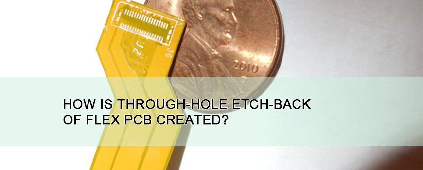
Two differ flex PCB impact through-hole etch-back
If you have read our articles about flex PCB board, you may find that its have very complex process.
This part we will discuss how is through-hole etch-back created.
Yes, most of those steps like normal metal core PCB etch process.
And there were many others different from those steps.
Simple to speak, through-hole etch-back is affected by two common flexible circuit fabrication processes.
The first one is micro-etch, then is the plasma etch technology.
The micro-etch technology of flex PCB
In micro-etch process, most of China flex PCB factories will submerge or sprayed process.
The aim is to remove a slight amount of copper on the substrate or base laminate.
This is not the micro-etch technology final aim.
If you have some knows about flex PCB constructions, you may know flex PCB ability related its connect and bending ability.
So we should improve plating adhesion ability to improve it’s bending and connect ability.
The drilling process of flex PCB board
Most of multilayer PCB board factories are laminated together several copper sheets.
Two reasons resulting drill various circuit layers at the same time.
The first reason is due to improve the effectiveness of flex PCB manufacture.
You know flex PCB production has million PCs have to drill.
If you just drill one by one, the time should cost very long.
Then we also want to ensure most flex PCB have the some holes, not only the hole size.
The positive through-hole etch-back of flex PCB
After the drill process, we should consider how to etching.
This sequence of flex PCB processing insures the copper surface of the hole is free from contaminants.
We also name this step as des-mearing.
Usually the plasma etch step appears this situation.
Due to plasma etch step can remove organic resins, such as smeared adhesives and dielectric debris.
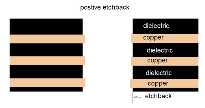
Through-hole etch-back more larer area can be plated
As we know plasma etch proce is to controlled to remove a specified amount of dielectric.
In other word, we shold cut some of the dielectric area and expose the copper layers.
Back to positive through-hole etch-back definition, only through etching or removing the dielectric arear, aim to expose the copper layer as larger as copper thickness.
So the through-hole etch-back tehcnologh can exposes more of the copper so a larger area can be plated.
In the theory, essentially three sides of the copper layer can now be plated.
This physical feature is used to create a more reliable plated through-hole.
Source:iconnect007