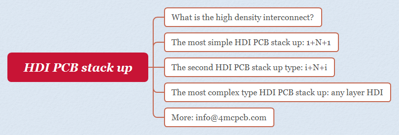
What is the high density interconnect?
This post is discuss HDI PCB stack up.
First of all, we want to discuss the definition of high density interconnect layers.
It’s a layer that very special, the connect function similar with conventional multilayer PCB.
But it’s very differ with the density, very high density in those layers.
So usually can’t not see on HDI PCB surface, until to testing or analytics the HDI PCB layers.
The most simple HDI PCB stack up: 1+N+1
Here we say simple is compare other HDI PCB board.
In fact, even this type HDI PCB stack up is more complex than most multilayer PCB boards.
The name of three HDI PCB type doesn’t use widely, so we just use 1+N+1 to discuss.
It’s an HDI PCB board that contains 1 “build-up” of high-density interconnection layers.
If you want to learn more detail about this type, please contact us, then we will discuss this 1+N+1 HDI PCB stack up in another article.
The second HDI PCB stack up type: i+N+i
This type HDI PCB stack up is more complex than first one.
Not only the stack up number have increase, but also increase the complex of stack up.
In this HDI PCB stack up, microvia on different layers.
And some microvia may staggered or stacked in different layers, this is the most different with first type HDI PCB stack up.
If required copper filled stacked microvia, many HDI PCB design engineers will get in trouble.
Because most of copper filled stacked microvia in HDI PCB stack up is the most difficult design issue.
The most complex type HDI PCB stack up: any layer HDI
Last one, but not the least, any layer HDI stacks up PCB board.
All the layers of a PCB are high density interconnection layers.
You can just look it as the inter layer of above type HDI PCB stack up.
If you have asked an HDI PCB test engineer, he must tell you HDI PCB board stack up is allowed all conductors in any layer of the PCB to be interconnected freely with copper filled stacked microwave structures.
This means all layers can connect by microwaves.

