We have discussed the subject of blind bias and buried Vias.
This paper also related to those two HDI PCB holes.
But different definition introduce before, we want to introduce different topics about blind bias and buried vias.
You know the technology of the blind was buried Vias are more than decades developing.
Some HDI PCB designers have conflicting information on the blind bias and buried Vias.
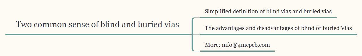
Simplified definition of blind vias and buried vias
If some green hands confused the definition of blind via or buried bias, please go back to read those two articles.
Here Emma just lists the simplified definition.
Blind Vias, a copper plated hole, connected inner layers and an outer layer, but does not go all the way through the HDI PCB.
Buried Vias, also a copper plated hole, connect inner layer and inner layer, the hole is completely internal or buried within the board.
The advantages and disadvantages of blind or buried Vias
We have discussed the advantage of the buried vias.
The main advantage is that design higher density HDI PCB to meet special requirement.
Also, there were some disadvantages to this HDI PCB technology.
First the design process is very complex.
Most of small rigid PCB manufacturers cannot produce HDI PCB.
Then is the cost of blind vias and buried was very expensive.
The cost of an HDI PCB using blind or buried vias is significantly higher than a conventional rigid PCB with the same number of layers.
4MCPCB experts introduce Blind and Buried Vias