Most green hands rigid PCB designers don’t know how to etch outer layer circuit.
That’s the reason why so many accidents during an etch circuit step.
Of course, this issue related to operator’s experience.
But many times depend rigid PCB designer’s skill, the etch circuit design process.
So 4MCPCB have to introduce the detail technology of etch rigid PCB outer layer process.
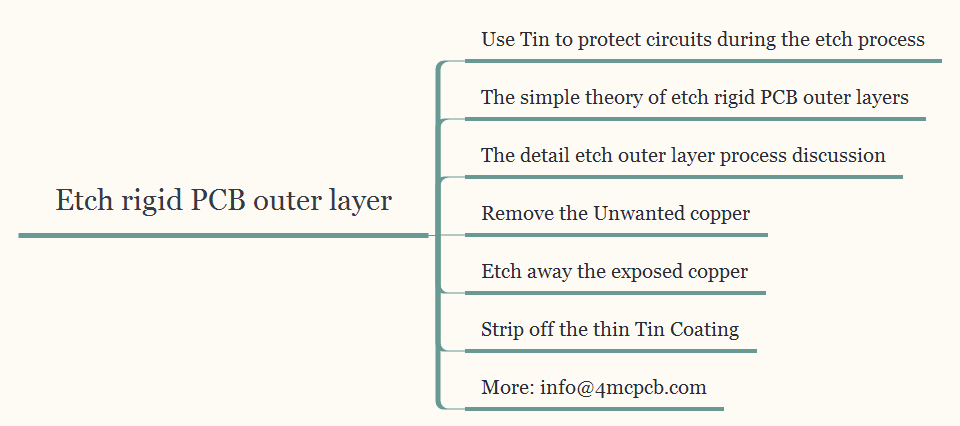
Use Tin to protect circuits during the etch process
Rich PCB Etch experts told Emma, most of China rigid PCB manufacturers will add a thin layer of Tin before the panel etch circuits.
So The top and the bottom copper are covered with this thin Tin layer.
The aim is to protect circuits, as an etch resist.
The simple theory of etch rigid PCB outer layers
We have know the copper is covered a thin Tin layer, as an etch resist.
So we want to etch the copper, just remove it from the surface.
This means the unwanted copper area the Tin material should be removed.
And the circuit area is protected with Tin material.
By the way, this process is a single continuous line.
We can easy to attach the images, or named circuits.
The detail etch outer layer process discussion
In this part, Emma wants to introduce three steps of etch outer layers.
Due to so many etch equipments use by different rigid PCB factory.
We will discuss the most normally etch rigid PCB outer layer method.
If you have any questions or want to learn more rigid PCB info, please mail to us.
Remove the Unwanted copper
Above we have mention that removes the thin Tin material to etch circuits.
In fact, this situation is the first step of etch outer layers.
The operators will dissolve and was off the resist.
Sometimes this step also can finish by auto machines.
So the unwanted copper area was exposed.
Etch away the exposed copper
4MCPCB rigid PCB experts told Emma, remove the unwanted copper is a chemical process.
Most of PCB designers will choose the powerful alkaline material to etch away the exposed copper.
There were some risk in etch away the exposed copper process, likely etch sideways.
So the key technology is carefully controlled to make sure etch the right area of the exposed copper.
That’s the reason why the finished conductor width design also very important.
Most green hands cannot understand this point very clearly.
The decades rigid PCB design should be aware that thicker copper foils need wider spaces between the tracks.
Strip off the thin Tin Coating
The last but not the least.
We have mentioned there was a thin Tin to protect the copper image.
In fact, this thin Tin coating just uses etch copper circuits process.
So we should trip off the thin Tin coating from the panel.
Then you can see that only designed copper pattern remains.
This means the tech rigid PCB outer copper circuits process have finished.
If you have any other question about etch copper process, please feel free to contact us.