We have discussed how to image the outer layers, is it similar process in image inner layer circuit?
Different flexible PCB engineers have differing opinions.
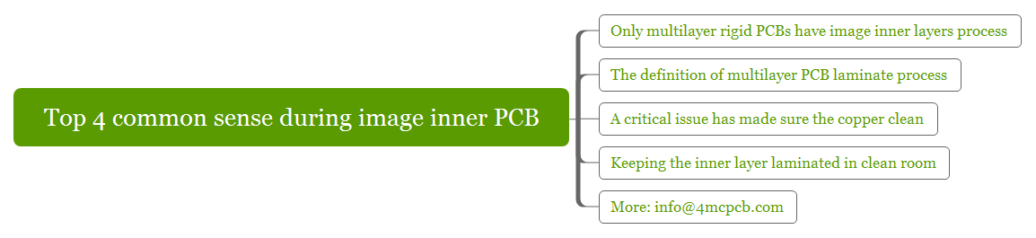
This paper will focus on Top 4 common sense during image inner PCB.
Only multilayer rigid PCBs have image inner layers process
You know most PCBs were through a panel laminate process.
One side or two side PCB manufacturing process, don’t need laminate step.
But in mot multilayer rigid PCB board, we should printed the inner circuits first, then printed outer layer circuit.
That’s the reason why only multilayer rigid PCBs have image inner layers process.
The definition of multilayer PCB laminate process
First of all, we should learn what is the multilayer PCB laminate.
We have introduced flexible circuit materials contain epoxy resin and glass-fibre.
In fact, these two PCB materials where the basic raw material for most of PCB types.
The multilayer PCB laminate process is basic raw material with copper foil pre-bonded onto each side.
This means the laminated process can be many times or separate each side one time.
Most of China rigid PCB factories used automotive machine to laminate the board.
A critical issue has made sure the copper clean
Most of the PCB plants has separate room to store copper raw material.
You know the copper material is very special PCB raw material.
The store room should keep good temperature and humidity.
This means must take more careful during the PCB copper material transfer.
Keeping the inner layer laminated in clean room
Usually an inner layer circuit laminated process in a clean room.
Because only in lean room can make sure no dust gets onto the surface inner circuit.
Or resulting a short or open circuit on the finish rigid PCB.