This paper will discuss the inspection of inner layers.
Many purchase doesn’t know the detail inspection process of inner layers.
Of course, Emma also don’t want all guys go to research the technology of inspection of the inner layer.
We want to more engineers or designers to know more the detailed inspection of inner layers.
When should we inspect inner layer circuits?
This is a very simple point for inspecting process, but also have some green hands don’t know.
When the inner core circuit layers were complete, we should arrange inspecting process.
Not some guy say when all multilayer rigid PCB board finish.
In the final testing process, we named final inspection, or electronic testing process.
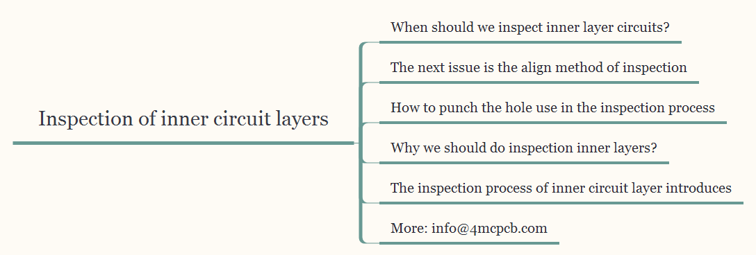
The next issue is the align method of inspection
In most multilayer PCB factories, use holes to align in mass production.
So the first step we should registration holes, and there were many meth to registration.
4MCPCB experts told Emma that use punch holes are used widely.
Because the use punch hole method is the most economical effective solution.
How to punch the hole use in the inspection process
There was a kind of punch machine named the optical punch.
The worker, load the inner circuit layer into the optical punch machine.
Then the machine lines up the registration targets in the copper pattern.
This means the punch machine will registration holes after punching.
Why we should do inspection inner layers?
This also a very simple issue, but may ignore by some new PCB guys.
The main reason is to avoid to any mistakes, make sure meet customers’ requirements.
You can image that when you multilayer PCB have all finish, and prepare to assembly component.
This time you find some mistakes in inner layer circuits.
Or you don’t know any problems with your multilayer PCB in inner circuit layers.
Then you assembly all components, but the end products cannot work.
What are you planning to handle this issue?
So, from the avoid mistakes point, all inner PCB layers should through the inspection process.
The inspection process of inner circuit layer introduces
Most of multilayer PCB plant will use an automatic machine to finish this process, like the automatic optical inspection system.
The inspection machine scans the inner PCB board in board strips.
Then it will compare it with the digital image generated from the original design data.
The original design data was designed by multilayer PCB designers, but not the customers original data.
If there are any errors, the machine will show it, displayed on screen.