Previous post we have discussed the solder mask costing process.
Our rigid PCB experts told Emma, there were some other steps to finish the solder mask.
So this paper will discuss some related theory of solder mask process.
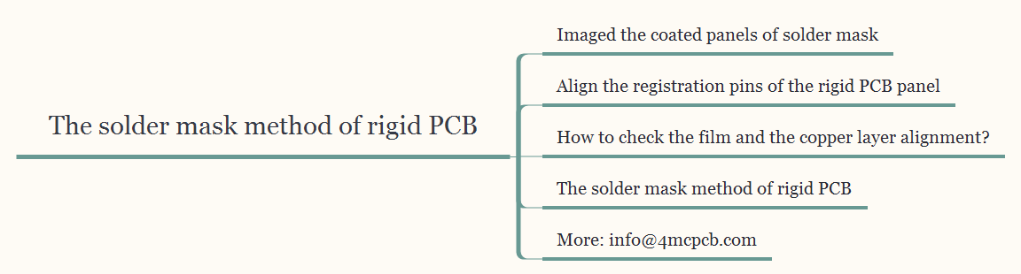
Imaged the coated panels of solder mask
The imaged method through drawer UV printer.
If you have know the traditional image photo process, you may understand the rigid PCB solder mask process more easy.
Align the registration pins of the rigid PCB panel
Small rigid PCB manufacturers have many issues, and then align the registration pins is the one.
If you have visited a bigger PCB plant, the align registration pins process handle by most green hands.
Because all of the operation processes followed SOP document.
The worker mounts the phototool films on the machine.
Then follow rigid PCB solder mask SOP, places the panel onto the registration pins.
How to check the film and the copper layer alignment?
Above we have known the alignment of the film and the circuit layer.
Then Emma wants to discuss the check rule.
A good align check rule is make sure the film and the copper layer are precisely aligned.
Usually, our 4MCPCB experts suggest the mask alignment will be better than 50 microns.
The solder mask method of rigid PCB
In fact, most of the solder mask method theory is the same.
The UV lamps in the machine harden the ink where the film is clear.
And the hardest area, we need a solder mask on the rigid PCB surface.