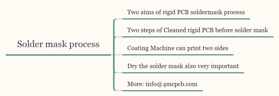
Two aims of rigid PCB soldermask process
You know most rigid PCB has an epoxy-ink solder mask printed onto each side.
The firstly aim is protecting the copper surface of rigid PCB.
Because the copper surface may be damaged in some bad situation.
The secondly aim is to prevent solder shorting between components during assembly rigid PCB.
If you have visit rigid PCB assembly plant, you may know the components should be careful assembly of the board.
The detail solder mask process introduce
Two steps of Cleaned rigid PCB before solder mask
In fact, each of rigid PCB manufacturing processes, the first step is a clean process.
Because all rigid PCB should be clean.
In cleaned rigid PCB step, the panels brushed to remove any surface tarnish.
Then the panels of rigid PCB will be conveyed into the yellow room.
You can understand this step as the second clean step.
Because each panel gives a final clean to remove any dust from the surface.
Then loaded into to the vertical coster.
Coating Machine can print two sides
Emma wants to clear that not each rigid PCB solder mask machine was working some method.
Most of big rigid PCB factories the coating machine can print both sides of the panel.
This means just one time can cover two sides with the epoxy soldermask ink.
The benefit of the coating machine is ensured the ink completely encapsulates the copper tracking.
The thickness of solder mask typically ranges from 35 to 40 microns.
In fact, this solder mask method can coating higher thickness than traditional method.
Dry the solder mask also very important
Most green hands think it’s so easy to solder mask.
Just keeping the printed solder mask on the rigid PCB, this process is over.
In fact, all solder makes rigid PCB should through dry process.
Because only dry solder masks can protect circuit layer.
That’s the reason most big rigid PCB manufacturers will arrange the worker check.
The operator checks for a complete and even coating.

