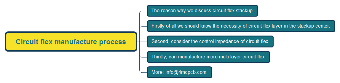
The reason why we discuss circuit flex stackup
This paper will discuss circuit flex stackup.
If you have read our shared article about circuit flex manufacture process, you will find it’s more simple than multilayer rigid PCB board.
But it’s also have difficult to design a good circuit flex stackup for most green guys.
How to place the circuit flex layer in the center of of the stackup?
Due to circuit flex stackup is so important, affect all design factors.
Firstly of all we should know the necessity of circuit flex layer in the stackup center.
If you have visited a circuit flex plant, you will find it’s very flexible.
This means there were damage circuit flex layer during the manufacturing process.
How to protect the circuit flex layer?
Most circuit flex manufacturers will putting circuit flex layers on the inside of the stackup.
One reason can help protect from exposure to outer layer circuit plating.
And the second factor considers circuit flex layer hold method.
Because circuit flex layers are so flexible to keep it statics.
Second, consider the control impedance of circuit flex
In previous article we have discus circuit flex design rule.
The control impedance is main factor related to flex circuit trace design.
To place circuit flex in center of stackup can simplifies the manufacturing process.
Most important is that improves circuit flex control impedance performance.
This means the electronic performance of circuit flex have improved.
Thirdly, can manufacture more multi layer circuit flex
During the circuit flex manufacturing processes were very complex.
We have know place circuit flex layer in the insider of the stackup can simplifies manufacturing processes.
Rich circuit flex designers use this to design multilayer circuit flex.
Those multilayer circuit flex layers can be etched away from the design as part of a separate process, allowing for more protection.