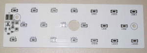
We have introduced many articles about the multilayer PCB manufactured process.
If you haven’t read any one, David recommend you go back to learn our unique explain to multilayer PCB.
This post will focus on how does a multilayer PCB hole work.
As same as before, David don’t want to just list some PCB terminology.
Is there possible to see via at the surface of multilayer PCBs?
We have known the construction of multilayer PCBs were different from 1 layer or 2 layer PCB boards.
If you look the surface of 2 layer PCB, you may notice there are so many holes on the surface.
But if you look a multilayer PCB, even though also there were some hole, but you can’t see was at the surface.
The theory of the multilayer PCBs hole working
Connect difference layer is the main function of multilayer PCBs hole.
If you have visited a multilayer PCB factory, you will find they will produce the inner layer hole, and then to laminated outer layers.
That’s the reason why you can see and via at the surface of multilayer PCB.

