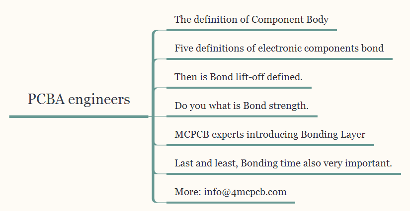
In this paper, we are going to discuss some skills of PCBA engineers should be known.
May some friends say, as a PCB manufacturer should be introduce more multilayer PCB technology.
In fact, most PCBA engineers know little PCB manufacturing technology.
PCBA is short for Printed Circuit Board Assembly.
The definition of Component Body
In PCBA process, use component assembly on the bare PCB board.
So, what is the definition of component body?
In professional PCB designer theory, the component is the portion of an electronic component, but exclusive of its pins or leads.
There were many kinds of PCB components, and different products have differed component requirement.
Five definitions of electronic components bond
Firstly, PCBA engineers should know Bond Interface.
Bond Interface is a common area on the PCB components.
This area is a leader and a land to which it has been terminated.
So, you can simple look a bond interface as a special connect method.
Then is Bond lift-off defined.
Simplely say Bond Lift-off is a failure condition.
And the lead is separated from the bonding surface.
The PCBA testing engineers may use this definition very often.
Do you what is Bond strength.
If you have seen a force per unit area, most new PCB guys don’t know this unit.
4MCPCB experts told Emma that Bond strength is a bond strength unit.
The force perpendicular to a board’s surface required to separate two adjacent layers of the board.
4MCPCB experts introducing Bonding Layer
This is an adhesive use in multilayer lamination processes.
As we know the adhesive function is bonding together other discrete layers of multi-layer printed board.
If you have read our raw PCB material article, in some word bonding layer similar with PPE.
Last and least, Bonding time also very important.
Bonding time is a duration process, and most of time depends on PCB manufacturer experience.
It’s from hot-bar-heat-up until the solder joint is completed, this duration can be finished.
As we know that during the Bonding time the hot-bar contact with lead and pad.
This means that it’s can effective PCB performance.

