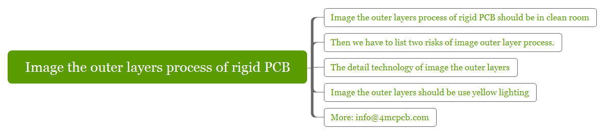
Image the outer layers process of rigid PCB should be in clean room
If you visit a professional rigid PCB factory, you must find many processes in clean room, likely image the outer layer process.
But why we should take this step to clean room, or the risk of image outer layer circuit process?
We have asked those questions to our 4MCPCB experts, and Emma summarize some tips below:
The first reason is that clean room can make sure no dust get onto the panel surface.
If your image outer layer process can’t keep very clean, there were some risks happen.
Then we have to list two risks of image outer layer process.
You know all rigid PCB manufacturers don’t want to two situations, short or open circuits.
Yes, those two points also the top risk during image outer layer process.
Our rigid PCB experts told us that, during the early days, there were occurred numbers of short or open circuits on the finished PCB boards.
So most of PCB manufacturers operate image the outer layer process in clean room.
The detail technology of image the outer layers
First step coated photosensitive film onto the copper.
You know all rigid PCB manufacturing method is chemical.
If you learn some articles, you can read many chemical keywords, likely photosensitive film in this part.
This is a kind of photoresist, and sensitive to UV light.
Now most PCB factories use hot-rolled method coated the photosensitive film onto the copper.
Then, using a cut-sheet laminator by an automatic rack.
In fact, this step is very simple, using special method coated photosensitive film onto the copper.
Image the outer layers should be use yellow lighting
In fact, this factor related to the photosensitive film characteristics.
Because all photosensitive films were sensitive to UV light.
So the PCB designers use yellow lighting to operate this step.
That’s the reason why almost all clean rooms in the PCB factory were yellow color.