We have introduced some common sense of image circuits.
If you just a new guy for PCB, please read previous article firstly.
It can help you understand the image outer layer circuits technology more easy.
Or you can contact 4MCPCB experts to ask some related questions.
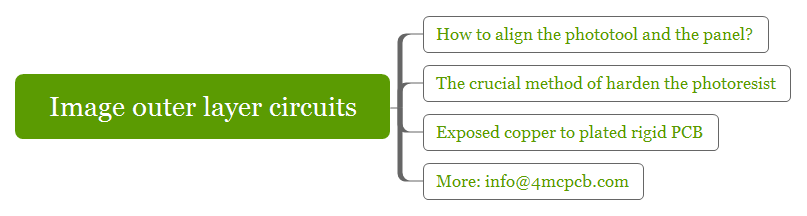
How to align the phototool and the panel?
This is a very professional technology issue.
There were some different method to align the phototool and the panel.
Emma wants to introduce a more normal type, use pin to fix the photo tool.
You know the bed of the printer have registration pins matching.
In this way, to align the phototool and the panel is the best economy method.
By the way, the phototool align must laminated one layer by one layer.
This the laminate way means very important.
4MCPCB expert told Emma, most of rigid PCB manufacturers will load the film onto the film on the top and bottom of the laminated panel.
So the middle layer is the laminated panel, it can protect very well.
The align effective is depend on the top and bottom layers are precisely aligned.
The crucial method of harden the photoresist
After aligning the phototool and the panel, we should consider how to harden the photoresist.
Because only the harden photoresist can protect the circuit trace.
The crucial method uses powerful UV lamps.
If you have know the theory of image outer circuit layers, you may know the photomask harden area depends on Gerber file.
The Mylar film, which protected the photoresist is removed.
The imaged panel is conveyed out of the clean room and through a developer which removes the unhardened resist.
For inner layer the copper pattern we want was covered by the resist.
Exposed copper to plated rigid PCB
The operator checks the panels to make sure that the copper surface is clean.
Most important is that all the unwanted resist has been removed.
After image outer layers, we should expose to plating.
So keeping clean of the panel surface finish is also the crucial factor.